My Expertise
- Scanning Probe Microscopy in variable environments and parameter spaces, including instrument development
- Advanced Functional Materials (complex oxides, van der Waals (2D) materials, halide perovskites, quantum materials, ...)
- Domain walls, skyrmions and other topological structures in ferroic materials
- Light interaction with materials at the nanoscale
A more detailed description of the research can be found on the Seidel Research Group website.
Fields of Research (FoR)
Functional Materials, Nanoscale Characterisation, Optical Properties of Materials, Electronic and Magnetic Properties of Condensed Matter; SuperconductivityBiography
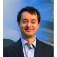
Jan Seidel is a professor in the School of Materials Science and Engineering, UNSW Sydney. He received his doctorate from TU Dresden, Germany in 2005. Prior to joining UNSW, Jan held positions at UC Berkeley, Lawrence Berkeley National Laboratory, and he was a visiting fellow at the University of Oxford. He has authored over 200 peer-reviewed papers with more than 16,000 citations and he has an h-index of 50.
His group has a focus on advanced...view more
Jan Seidel is a professor in the School of Materials Science and Engineering, UNSW Sydney. He received his doctorate from TU Dresden, Germany in 2005. Prior to joining UNSW, Jan held positions at UC Berkeley, Lawrence Berkeley National Laboratory, and he was a visiting fellow at the University of Oxford. He has authored over 200 peer-reviewed papers with more than 16,000 citations and he has an h-index of 50.
His group has a focus on advanced scanning probe microscopy for the study of physical properties of novel materials, particularly transition-metal oxides, 2D materials and hybrid halide perovskites, in the forms of thin films, nanomaterials and nanoscale devices. His research targets a wide range of optoelectronic, data storage and energy related technology, including nonvolatile memories, solar cells and nanoelectronics.
Jan's group has openings for PhD students. Anyone interested should send a CV to jan.seidel@unsw.edu.au.
Positions held
- University of New South Wales, 2012-present
- University of Oxford, Visiting Fellow, 2016
- Lawrence Berkeley National Laboratory, Research Scientist, 2008-2011
- University of California, Berkeley, Research Associate, 2006-2007
- University of Technology Dresden, Research Associate, 2001-2006
- Leibniz Institute for Solid State and Materials Research (IFW), Research Intern, 1997
Expertise
ferroelectrics, multiferroics, photovoltaics, scanning probe microscopy, domain structures, domains, topological defect, topological insulators, 2D van der Waals materials, optics and photonics, nanostructures, nanotechnology, nanostructured materials, nanoscience & nanotechnology, organic semiconductors, infrared spectroscopy of semiconductors, atomic force microscopy, scanning tunneling microscopy (stm) lit, piezoelectric materials, piezo-response force microscopy, magnetic properties, magnetoelectric, metal oxides, pulsed laser deposition, material interfaces, biomaterials, electron microscopy, neutron scattering, quantum measurement, neuromorphic engineering, machine learning, fourier transform infrared spectroscopy, nanolithography, xrd, thin films, transition metals, materials science
- Advanced scanning probe microscopy applied to materials characterisation (AFM, c-AFM, PFM, EFM, MFM, KPFM, STM/STS, nano-IR, …)
- Domain walls, skyrmions and other topological structures in ferroic materials
- Oxide nanoelectronics, interfaces in complex oxides
- Ferroelectric and multiferroic materials
- 3rd generation photovoltaic, thermoelectric, and electrochromic materials, e.g. halide perovskites
- Quantum materials
- Nanoscale phases and properties of materials, 2D materials
- Inorganic / organic semiconductors, biomaterials
- Nano-optics and spectroscopy, plasmonics
- X-ray based synchrotron techniques (XAS, XMCD and XMLD-PEEM)
- High-resolution transmission electron microscopy (TEM) and spectroscopy (EELS)
- Neutron scattering
My Awards
- UNSW Outstanding Research Supervisor Award, 2019
- Arc Postgraduate Council Supervisor Award, 2018
- Arc Postgraduate Council Supervisor Award, 2017
- Visiting Fellowship, St. Catherine's College, University of Oxford, 2016
- Visiting Fellowship, Materials Department, University of Oxford, 2016
- Endeavour Executive Fellowship, Australian Government, 2016
- Travel award, The Royal Society, 2016
- Theo Murphy Australian Frontiers of Science travel award, Australian Academy of Science, 2015
- Future Fellowship, Australian Research Council, 2011
- Feodor Lynen Fellowship, Alexander von Humboldt Foundation, 2006-2010
- Graduate Fellowship of the German National Science Foundation (DFG), 2001-2004
My Research Activities
Professor Seidel’s research interests in the area of advanced electronic, photonic and spintronic materials include the following:
- Advanced scanning probe microscopy applied to materials characterisation (AFM, c-AFM, PFM, EFM, MFM, KPFM, STM/STS, nano-IR, …)
- Domain walls, skyrmions and other topological structures in ferroic materials
- Oxide nanoelectronics, interfaces in complex oxides
- Ferroelectric and multiferroic materials
- 3rd generation photovoltaic, thermoelectric, and electrochromic materials, e.g. halide perovskites
- Quantum materials
- Nanoscale phases and properties of materials, 2D materials
- Inorganic / organic semiconductors, biomaterials
- Nano-optics and spectroscopy, plasmonics
- X-ray based synchrotron techniques (XAS, XMCD and XMLD-PEEM)
- High-resolution transmission electron microscopy (TEM) and spectroscopy (EELS)
- Neutron scattering
A more detailed description of the research can be found on the Seidel Research Group website.
My Research Supervision
Supervision keywords
Areas of supervision
- Advanced scanning probe microscopy applied to materials characterisation (AFM, c-AFM, PFM, EFM, MFM, KPFM, STM/STS, nano-IR, …)
- Domain walls, skyrmions and other topological structures in ferroic materials
- Oxide nanoelectronics, interfaces in complex oxides
- Ferroelectric and multiferroic materials
- 3rd generation photovoltaic, thermoelectric, and electrochromic materials, e.g. halide perovskites
- Quantum materials
- Nanoscale phases and properties of materials, 2D materials
- Inorganic / organic semiconductors, biomaterials
- Nano-optics and spectroscopy, plasmonics
- X-ray based synchrotron techniques (XAS, XMCD and XMLD-PEEM)
- High-resolution transmission electron microscopy (TEM) and spectroscopy (EELS)
- Neutron scattering
My Engagement
- Member, ARC College of Experts, 2024-2026
- Member of the Academic Board, UNSW
- Research Director, School of Materials Science and Engineering
- Advisory Board, Advanced Electronic Materials (Wiley)
- Editorial Board, Materials Today Electronics (Elsevier)
My Teaching
- MATS6008 Advanced Functional Materials, UNSW, 2020-
- NANO3001 Advanced Nanomaterials, UNSW, 2013-2020
- Mentor, Center for Energy Efficient Electronics Science (E3S), UC Berkeley, USA, 2011
- Mentor, Center of Integrated Nanomechanical Systems (COINS), UC Berkeley, USA, 2009
- Teaching Assistant, Institute of Applied Photophysics, TU Dresden, Germany, 2001-2004
Location
Hilmer Building (E10), Room 340
University of New South Wales
Sydney NSW 2052