Site Maintenance will take place from 4:00 PM on 2024-04-29 to 9:00 AM on 2024-05-01.
Please do not make any content change during this time, otherwise all the changes will be lost.

Find a researcher

Find your prospective supervisor, research project or research group, collaborator or expert by searching UNSW Sydney Researcher Profiles. Use keywords to view their research interests, publications and areas of expertise.

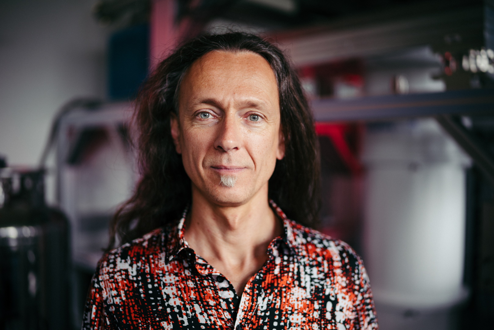
Professor Jan Seidel

Faculty: Science
Fields of Research (FoR): Functional Materials, Nanoscale Characterisation, Optical Properties of Materials, Electronic and Magnetic Properties of Condensed Matter; Superconductivity

Jan Seidel is a professor in the School of Materials Science and Engineering, UNSW Sydney. He received his doctorate from TU Dresden, Germany in 2005.
Dr Wayne Hutchison

Faculty: UNSW Canberra
Fields of Research (FoR): Electronic and Magnetic Properties of Condensed Matter; Superconductivity, Environmental Nanotechnology, Condensed Matter Characterisation Technique Development, Quantum Information, Computation and Communication

Scholarships of $35,000 (AUD) are available for PhD students who achieved H1 /High Distinction in their UG program and/or have completed a Masters by Research.
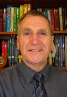
Dr Oleh Klochan

Faculty: UNSW Canberra
Fields of Research (FoR): Condensed Matter Physics, Electronic and Magnetic Properties of Condensed Matter; Superconductivity, Nanoelectronics, Quantum Physics
SEO tags:

Graduated from Ivan Franko National University (Lviv, Ukraine) in 2000 majoring in Physics of Semiconductors (M.Sc. equivalent) PhD in Condensed Physics from UNSW (2003-2007), QED group.
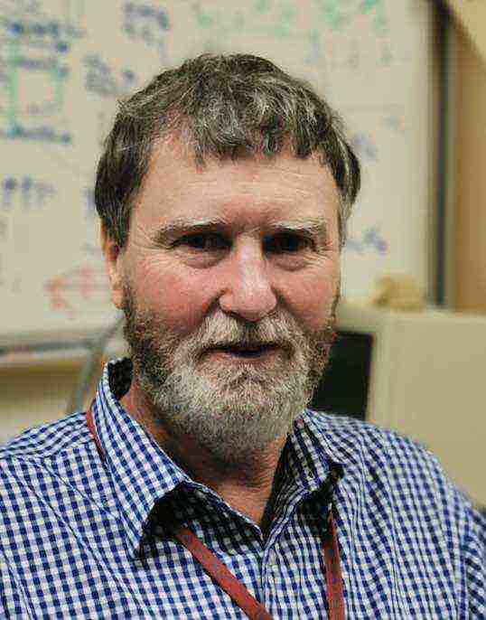
Associate Professor Glen Alan Stewart

Faculty: UNSW Canberra
Fields of Research (FoR): Condensed Matter Physics, Electronic and Magnetic Properties of Condensed Matter; Superconductivity

Glen has a BSc (Honours), PhD in Physics and a Dip. Ed. from Monash University.
Building up quantum electronics with tailored semiconductor nanostructures

Field of Research (FoR):
SEO tags:

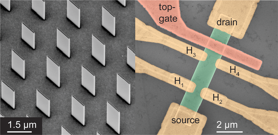
This project aims to develop a new generation of nanoscale InAs/GaSb devices produced ‘from the bottom up’ using state-of-the-art 3D templated semiconductor growth methods. This material’s key feature is a pair of electron and hole layers separated by a few nanometers.