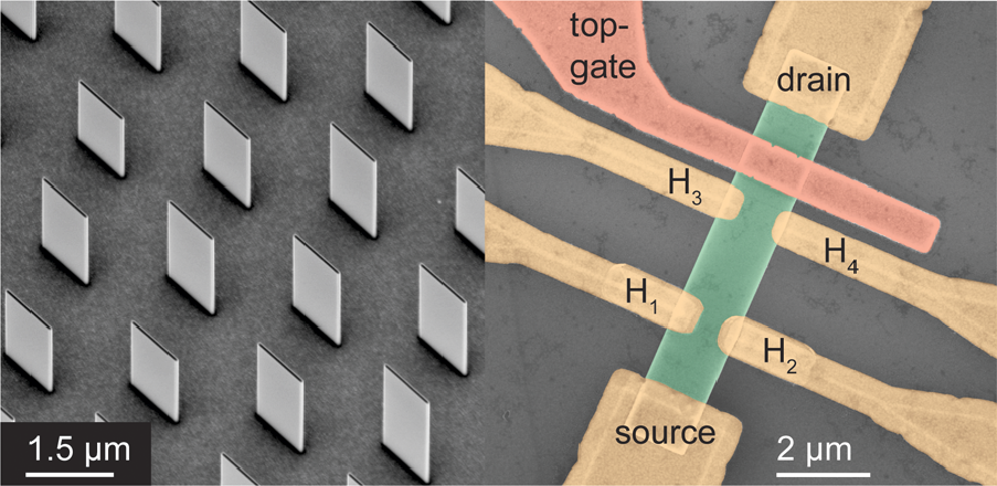
This project aims to develop a new generation of nanoscale InAs/GaSb devices produced ‘from the bottom up’ using state-of-the-art 3D templated semiconductor growth methods. This material’s key feature is a pair of electron and hole layers separated by a few nanometers. These provide access to novel states of matter such as exciton condensates and topological insulators with potential applications in quantum information technologies. The project’s innovation is to template growth to give devices where the InAs/GaSb interface sits perpendicular to the device plane. This will enable independent contact to the electron and hole layers for the first time, opening new avenues of research and technology development for this material.
Building up quantum electronics with tailored semiconductor nanostructures
ARC Discovery Project DP170102552
